Molecular Lego for nanoelectronics

FAU Forschungskollaboration zwischen Exzellenzcluster und Sonderforschungsbereich
The ability to assemble electronic building blocks consisting of individual molecules is an important objective in nanotechnology. An interdisciplinary research group at FAU is now significantly closer to achieving this goal. The team of researchers headed by Prof. Dr. Sabine Maier, Prof. Dr. Milan Kivala and Prof. Dr. Andreas Görling has successfully assembled and tested conductors and networks made up of individual, newly developed building block molecules. These could in future serve as the basis of components for optoelectronic systems, such as flexible flat screens or sensors. The FAU researchers have published their results in the journal Nature Communications.
Lithographic techniques in which the required structures are cut from existing blocks are mainly employed at present to produce micro- and nano-electronic components. ‘This is not unlike how a sculptor creates an object from existing material by cutting away what they do not need. How small we can make these structures is determined by the quality of the material and our mechanical skills,’ explains Prof. Dr. Sabine Maier from the Chair of Experimental Physics. “We now have something like a set of Lego bricks for use in the nanoelectronic field; this enables us to fabricate the required objects ‘bottom-up’, in other words, we start from the base and place the tiny units one on top of the other.”
The researchers can now use these building blocks to produce the smallest one-dimensional structures –conductors – and two-dimensional structures –networks – under precision-controlled conditions. The structures are characterised by their extreme regularity with no structural flaws. Flawless structures of this kind are essential for producing minuscule nanoelectronic components with various properties.
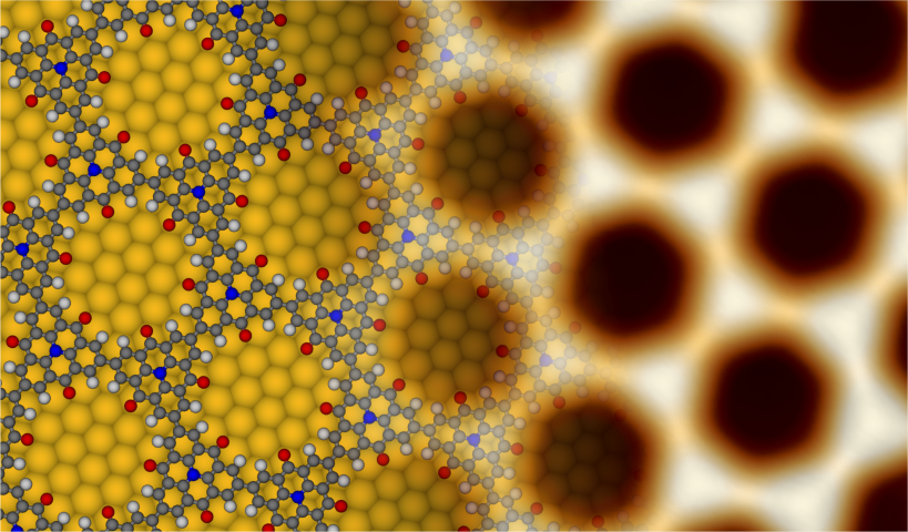
The basis of these synthetic organic semiconductors – the Lego bricks as it were – was synthesised at the Institute for Organic Chemistry at FAU. ‘Our basic building block is a triangle consisting of 21 carbon atoms with one nitrogen atom at its centre, with either hydrogen, iodine or bromine deposited at the corners depending on the desired structure’ clarifies Prof. Dr. Milan Kivala from the Chair of Organic Chemistry I. The FAU researchers attach the corresponding molecules to a carrier surface made of gold and this is then heated to 150 – 270°C. This process initially forms hexagons or chains. When the samples reach a temperature of 270°C, the molecular building blocks form chemically bound, flat and honeycomb-like meshes that are similar in structure to that of the Nobel Prize-winning material graphene.
The research group has already managed to determine one of the major electrical properties – the so-called ‘band gap’. ‘We have established that the band gap of two-dimensional structures is smaller than that of one-dimensional arrangements of the same molecular building blocks,’ adds Prof. Dr. Andreas Görling from the Chair of Theoretical Chemistry. ‘These insights will help us in the future to predict the properties of these structures and adjust them to the desired values for specific optoelectronic applications.’
This research has opened up the possibility of fabricating ever-smaller nanoelectronic components. The current lithographic techniques used in the commercial production of microchips can only create structures larger than 14 nanometres. The conductors generated in Erlangen are only a little wider than one nanometre and therefore around fifty thousand times thinner than a human hair. However, a number of additional developments are necessary before they can be used in technological applications. For example, it is still necessary to find a suitable electrically non-conductive carrier material.
The results stem from an interdisciplinary collaboration within the Cluster of Excellence ‘Engineering of Advanced Materials’ and the Collaborative Research Centre 953 ‘Synthetic Carbon Allotropes’ which has been published in an open access article entitled “Hierarchical on-surface synthesis and electronic structure of carbonyl-functionalized one- and two-dimensional covalent nanoarchitectures” in the scientific journal Nature Communications 8, 14765 (2017). (doi: 10.1038/ncomms14765.
Read the full article at www.nature.com/articles/ncomms14765

Kontakt
Prof. Dr. Sabine Maier
Tel.: 09131/ 85 27268
sabine.maier@fau.de